이 매뉴얼은 JK전자(JK Electronics) 에 의해서 번역, 수정, 작성 되었고 소유권 또한
JK전자(JK Electronics)의 것입니다. 소유권자의 허가를 받지 않고 무단으로 수정, 삭제하거나 배포 할 수 없습니다.
S5PV210 StartKit 하드웨어
* Update history
- 2011.12.21 : 초기 Release
2011.12.26 S/W 업데이트
1. S5PV210 StartKit 개발보드
2. S5PV210 StartKit interface description
3. S5PV210 BOOT Memory layout
1. S5PV210 StartKit 개발보드
1.1 Cortex-A8 개요Cortex-A8 application processor 는 ARMv7 architecture 에 기반을 두고 있습니다. ARM의 Cortex-A8 는 600MHz ~ 1GHz 클럭 성능으로 동작하는 아주 강력한 프로세서 입니다. A8 프로세서는 다양한 모바일 디바이스 기기들에서 사용하기에 적합 하도록 2000MIPS의 속도로 동작할때 300mW 이하 정도의 전력을 소모합니다.또한 A8 프로세서는 코드 효율성과 성능 개선을 위해서 새로운 기술이 적용되었습니다. 그것은 바로 Media 처리 속도 개선을 위해서 NEON 과 signal rocessing, Jazelle RCT(can support JAVA program of pre-compiled and real-time compilation) 기술이 포함되어진 것입니다. 그리고 Artisan Advantage-CE 라는 새로운 Library는 abnormal processing 성능과 전력소모를 줄이도록 하였습니다.
1.2 Cortex-A8과 ARM11의 비교
(1) Cortex-A8
- ARMv7 instruction based architecture
- Running speed up to 600MHz to 1GHz
- 300mW power consumption in the running
- Pipeline architecture is based on double complex symmetric and 13-stage pipeline with advanced dynamic branch prediction to achieve 2.0 DMIPS/MHz
- 10 NEON media pipeline
- Dedicated L2 cache, with programmable wait state, and L3 support multiple outstanding transactions between the memory to take advantage of CPU.
(2) ARM11
- Based on the ARMv6 instruction architecture
- Operating frequency 300MHz-500MHz, in 0.13um process, 1.2v conditions
- ARM11 processor power consumption as low as 0.4mW/MHz.
- ARMv6 architecture in the past to maintain all the T(Thumb instructions) and E(DSP instructions) extension.
- ARM11 processor pipeline composed by the 8-stage pipeline. But there is no dedicated L2 cache, compared to the Cortex-A8, a lot of processing power will be weak.
1.3 H/W 사양
(1) Samsung A8 processor 1GHz S5PV210
(2) 512 MByte DDRII memory, 256M byte SLC type NandFlash
(3) WM9713 Audio chip.
(4) DM9000AEP 100M network support
(5) Single PMIC WM8310 : intelligent power management, support for dynamic voltage adjustment charge and DVS
(6) 230pin MCU TQFP package, most of the interface leads
(7) Only 6cm*6cm, suitable for embedded devices
(8) The core board work at full speed 1GHZ, power about 5V/200mA
| CPU Board Features | |
| CPU | Samsung S5PV210 1GHz support NEON |
| SRAM | 4G bits(512 MBytes) DDR2 SRAM |
| Flash | 2G bits(256 MBytes) SLC NAND FLASH |
| PMIC | Integrated single-chip power management chip WM8310 |
| Ethernet | DM9000AEP 100M network |
| Audio | WM9713 |
| Pin Type | 230pin MCU TQFP package |
| Size | 60mm*60mm |
| Power | Power about 5V/200mA |
1.3.2 Bottom 보드 사양
| Bottom Board Features | |
| RS232 | RS232 * 2, TTL * 2 |
| RS485 | One RS485 |
| CAN | One CAN interface |
| Camera | One 20Pin CMOS interface |
| AVIN | One TVP5150 AVIN interface(CCD 카메라 인터페이스 가능) |
| Ethernet | DM9000AEP 100M network interface |
| Audio | Mic input, Line In(3.5파이), Speaer Out(2Pin), Headset Out(3.5파이) |
| TV Out | One TV Out |
| HDMI | One HDMI Out |
| VGA Out | One VGA(Chrontel) Out |
| LCD | 2*RGB Interface(50핀 FPCB, 커넥터형), 7인치, 10인치 사용가능 |
| USB Host, OTG | 2*USB 2.0 Host, 1*USB OTG |
| KEY | 8x8 matrix keypad, 5*User Key |
| SDIO Wifi | One SDIO Wifi interface |
| RTC | One RTC |
| JTAG | 20Pin JTAG interface |
| 외부확장 인터페이스 | I2C, SPI, PWM, AD/DA interface |
| SD Memory | One SDIO Memory interface |
| Power | USB전원과 5V DC 어댑터(외경:5.5mm, 내경:2mm) 전원 가능 |
| Size | 165mm*120mm(H*V) |
| 옵션 제품 | CDMA(Mini PCI), GPS(UART) Bluetooth(UART) Wifi(SDIO) Combo 모듈 사용가능 |
- Power Support
(1) Support 5V power input (DC5V 2pin)
(2) Support for battery input (VBAT 2pin)
(3) Support USB-power.
(5) Support the VBAT VUSB DC5V seamless switching, priority DC5V>VUSB>VBAT
(6) Support the switch machine keys detect
(7) 1.8 ~ 3V RTC backup battery input pin
- Display Interface
(1) RGB 24Bit Interface
(2) HDMI output
(3) TVOUT output
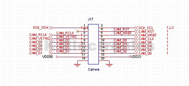
(4) TOUCH interface support
- System bus
(1) 16-bit data bus
(2) 2^16 address space
(3) Support the single-and double-byte read and write
- Camera Interface
(1) Support all the way Camera 8bit RGB or YUV input
- Serial Bus
(1) Two IIC interface
(2) TTL UART * 4, RS232(DB9) UART * 2
(3) Two SPI
(4) All the way USB HOST2.0
(5) All the way OTG2.0
- SDIO interface
(1) Two 4bit SDIO interface, which can be accessed SDIO device and SDMEMOY
- Network interfaces
(1) All the way to state network interfaces 100M
- Audio
(1) Supports two-way differential MIC input
(2) Support all the way to single-ended MIC input
(3) Support one headphone output (with insertion detection)
(4) Speaker support two differential outputs, adjustable output gain
(5) All the way to the left and right LINE inputs
- Keyboard interface
(1) 8*8 matrix Keyboard
(2) Can be used as GPIO
- External interrupt interface
(1) Supports the GPIO inputs and outputs, support for external interrupt
(2) 18 external interrupt into the support
- Configuration pins BOOT
(1) Support NAND and UART pin configuration
- JTAG
(1) Support for debugging emulator
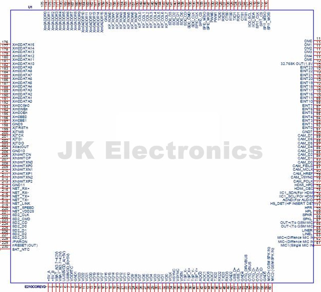
1.3.2 Definition of the core board pin
Pin No |
Definitions |
Functions |
Multiplexing funciton |
Pin No |
Definitions |
Functions |
Multiplexing funciton |
1 |
5V |
5V power supply input | 116 |
SPI1_MOSI |
SPI1 MOSI | ||
2 |
5V |
5V power supply input | 117 |
SPI1_MISO |
SPI1 MISO | ||
3 |
VBAT |
Battery input (3.7 to 4.2) | 118 |
SPI1_CS |
SPI1 CS | ||
4 |
VBAT |
Battery input (3.7 to 4.2) | 119 |
SPI1_CLK |
SPI1 CLK | ||
5 |
USBVDD |
USB powered 5V input | 120 |
IIC0_SDA |
|||
6 |
USBVDD |
USB powered 5V input | 121 |
IIC0_SCL |
|||
7 |
VDDRTC |
RTC power supply (1.8 ~ 3.0V) | 122 |
RTS1 |
Serial Channel 1 | ||
8 |
GND |
전원 GND | 123 |
CTS1 |
|||
9 |
VD23 | 24-bit RGB bus | 124 |
RXD1 |
|||
10 |
VD22 |
125 |
TXD1 |
||||
11 |
VD21 |
126 |
RTS0 |
Serial Channel 0 | |||
12 |
VD20 |
127 |
CTS0 |
||||
13 |
VD19 |
128 |
RXD0 |
||||
14 |
VD18 |
129 |
TXD0 |
||||
15 |
VD17 |
130 |
PWM1 |
||||
16 |
VD16 | 131 |
PWM0 |
||||
17 |
VD15 |
132 |
SPI0_MOSI |
SPI0 MOSI | |||
18 |
VD14 |
133 |
SPI0_MISO |
SPI0 MISO | |||
19 |
VD13 |
134 |
SPI0_CS |
SPI0 CS | |||
20 |
VD12 |
135 |
SPI0_CLK |
SPI0 CLK | |||
21 |
VD11 |
136 |
SD0_CLK | SDIO 0 interface | |||
22 |
VD10 |
137 |
SD0_CMD |
||||
23 |
VD9 |
138 |
SD0_CD |
||||
24 |
VD8 |
139 |
SD0_D0 |
||||
25 |
VD7 |
140 |
SD0_D1 |
||||
26 |
VD6 |
141 |
SD0_D2 |
||||
27 |
VD5 |
142 |
SD0_D3 |
||||
28 |
VD4 |
143 |
KP_COL7 |
Matrix keyboard | |||
29 |
VD3 |
144 |
KP_COL6 |
||||
30 |
VD2 |
145 |
KP_COL5 |
||||
31 |
VD1 |
146 |
KP_COL4 |
||||
32 |
VD0 |
147 |
KP_COL3 |
||||
33 |
VCLK |
Shows the clock signal | 148 |
KP_COL2 |
|||
34 |
HSYNC |
Horizontal scan signal display | 149 |
KP_COL1 |
|||
35 |
VSYNC |
Shows the vertical scanning signal | 150 |
KP_COL0 |
|||
36 |
VDEN |
DE signal display | 151 |
KP_ROW7 |
Matrix keyboard | ||
37 |
TSP_X- |
AIN2 |
152 |
KP_ROW6 |
|||
38 |
TSP_X+ |
AIN3 |
153 |
KP_ROW5 |
|||
39 |
TSP_Y- |
AIN4 |
154 |
KP_ROW4 |
|||
40 |
TSP_Y+ |
AIN5 |
155 |
KP_ROW3 |
|||
41 |
ADC0 |
ADC channel 0 | 156 |
KP_ROW2 |
|||
42 |
ADC1 |
ADC channel 1 | 157 |
KP_ROW1 |
|||
43 |
ADC6 |
ADC channel 6 | 158 |
KP_ROW0 |
|||
44 |
ADC7 |
ADC channel 7 | 159 |
GND |
|||
45 |
TXD2 |
160 |
Xm0ADDR15 |
Bus channel 0 address line | |||
46 |
RXD2 |
161 |
Xm0ADDR14 |
||||
47 |
TXD3 |
162 |
Xm0ADDR13 |
||||
48 |
RXD3 |
163 |
Xm0ADDR12 |
||||
49 |
GND |
Power GND | 164 |
Xm0ADDR11 |
|||
50 |
USB_D+ |
USB HOST D+ | 165 |
Xm0ADDR10 |
|||
51 |
USB_D- |
USB HOST D- | 166 |
Xm0ADDR9 |
|||
52 |
GND |
Power GND | 167 |
Xm0ADDR8 |
|||
53 |
OTG_DRVVBUS |
OTG external power supply enable signal | 168 |
Xm0ADDR7 |
|||
54 |
OTG_DVBUS |
OTG power signal | 169 |
Xm0ADDR6 |
|||
55 |
OTG_D- |
OTG D+ | 170 |
Xm0ADDR5 |
|||
56 |
OTG_D+ |
OTG D- | 171 |
Xm0ADDR4 |
|||
57 |
OTG_ID |
OTG ID signal | 172 |
Xm0ADDR3 |
|||
58 |
GND |
Power GND | 173 |
Xm0ADDR2 |
|||
59 |
MIC2+ |
MIC audio input channel2 + | 174 |
Xm0ADDR1 |
|||
60 |
MIC2- |
MIC audio input channel2 - | 175 |
Xm0ADDR0 |
|||
61 |
MIC1 |
Single-ended MIC input | 176 |
Xm0ADDR15 |
|||
62 |
MIC- |
MIC audio input channel1 + | 177 |
Xm0DATA14 |
|||
63 |
MIC+ |
MIC audio input channel1 - | 178 |
Xm0DATA13 |
|||
64 |
LINEL |
LINE left channel signal | 179 |
Xm0DATA12 |
|||
65 |
LINER |
LINE right channel signal | 180 |
Xm0DATA11 |
|||
66 |
OUT- |
Audio output - | 181 |
Xm0DATA10 |
|||
67 |
OUT+ |
Audio output + | 182 |
Xm0DATA9 |
|||
68 |
SPKL |
SPK left channel | 183 |
Xm0DATA8 |
|||
69 |
SPKR |
SPK right channel | 184 |
Xm0DATA7 |
|||
70 |
HPL |
Headphone left channel | 185 |
Xm0DATA6 |
|||
71 |
HPR |
Headphone right channel | 186 |
Xm0DATA5 |
|||
72 |
HS_DET |
Headphones into the test | 187 |
Xm0DATA4 |
|||
73 |
AUGND |
Audio GND | 188 |
Xm0DATA3 |
|||
74 |
IIC1_SDA |
HDMI IIC configuration data lines | Only available for the HDMI | 189 |
Xm0DATA2 |
||
75 |
IIC1_SCL |
HDMI IIC configuration data lines | Only available for the HDMI | 190 |
Xm0DATA1 |
||
76 |
HDMI_CEC |
HDMI CEC signal | 191 |
Xm0DATA0 |
|||
77 |
HDMI_HPD |
HDMI Plug Detect Signal | 192 |
Xm0CSn0 |
Xm0 channel chip select 0 | ||
78 |
CAM_PCLK |
CAM pixel clock signal | 193 |
Xm0WEn |
Xm0 write signal channel | ||
79 |
CAM_VSYNC |
CAMERA Column sync signal | 194 |
Xm0OEn |
Xm0 read channel signal | ||
80 |
CAM_HREF |
CAMERA line sync signal | 195 |
Xm0BE0 |
Xm0 channel low byte read | ||
81 |
CAM_MCLK |
CAMERA master clock signal output | 196 |
Xm0BE1 |
Xm0 channel 8-bit byte read high | ||
82 |
CAM_FIELD |
Reset signal for the CAMERA | 197 |
GND |
|||
83 |
CAM_D0 |
CAMERA data bus | 198 |
XjTRSTn |
JTAG Pins | ||
84 |
CAM_D1 |
199 |
XjTMS |
JTAG Pins | |||
85 |
CAM_D2 |
200 |
XjTCK |
JTAG Pins | |||
86 |
CAM_D3 |
201 |
XjTDI |
JTAG Pins | |||
87 |
CAM_D4 |
202 |
XjTDO |
JTAG Pins | |||
88 |
CAM_D5 |
203 |
DACOUT0 |
TV output signal | |||
89 |
CAM_D6 |
204 |
GND |
||||
90 |
CAM_D7 |
205 |
XhdmiTCN |
HDMI interface cable | |||
91 |
GND |
206 |
XhmdiTCP |
||||
92 |
EINT0 |
207 |
XhdmiTXN0 |
||||
93 |
EINT1 |
208 |
XhdmiTXP0 |
||||
94 |
EINT3 |
209 |
XhdmiTXN1 |
||||
95 |
EINT4 |
210 |
XhdmiTXP1 |
||||
96 |
EINT5 |
211 |
XhdmiTXN2 |
||||
97 |
EINT6 |
212 |
XhdmiTXP2 |
||||
98 |
EINT7 |
213 |
GND |
||||
99 |
EINT10 |
214 |
NET_RX+ |
Network Interface | |||
100 |
EINT11 |
215 |
NET_RX- |
||||
101 |
EINT16 |
216 |
NET_TX+ |
||||
102 |
EINT17 |
217 |
NET_TX- |
||||
103 |
EINT18 |
218 |
NET_LINK |
||||
104 |
EINT19 |
219 |
NET_SPEED |
||||
105 |
EINT20 |
220 |
NET_VDD25 |
||||
106 |
EINT21 |
221 |
SD2_CLK |
SD2 Interface | |||
107 |
EINT22 |
222 |
SD2_CMD |
||||
108 |
EINT23 |
223 |
SD2_CD |
||||
109 |
CLK_32.768K |
1.8V 32.768KHz output | 224 |
SD2_D0 |
|||
110 |
OM5 |
BOOT configuration pins | 225 |
SD2_D1 |
|||
111 |
OM4 |
226 |
SD2_D2 |
||||
112 |
OM3 |
227 |
SD2_D3 |
||||
113 |
OM2 |
228 |
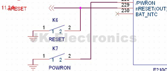
/PWRON |
Core board enable pin | |||
114 |
OM1 |
229 |
nRESET |
Reset output, active low | |||
115 |
OM0 |
230 |
BAT_NTC |
Battery temperature detection |
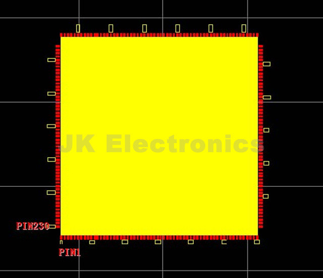
1.3.3 Package size of the core board LAYOUT
2. S5PV210 StartKit interface description
2.1 S5PV210 StartKit 하드웨어 상세 설명
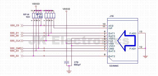
(1) SD0 card interface circuit (such as no need for WINCE)
(2) UART 포트
PC와 통신시 시리얼 케이블은 2, 3번핀은 크로스된 케이블을 사용하시기 바랍니다.
USB to 시리얼 케이블 사용시 반드시 제품과 함께 제공되는 시리얼 연장 케이블을 연결해서 사용하시기 바랍니다.
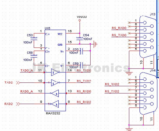
또한 UART0를 아래와 같이 DIP스위치의 설정에 따라서 다른 용도로 사용할 수 있습니다.
* UART0 DIP 스위치
UART0 |
1 |
2 |
3 |
4 |
5 |
6 |
7 |
8 |
RS232(DB9) Level |
On |
On |
||||||
TTL Level |
On |
On |
||||||
RS485(DB9) |
On |
On |
||||||
Bluetooth |
On |
On |
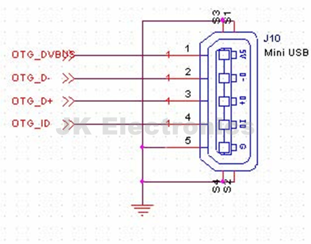
(3) OTG interface
(4) Power supply
반드시 5V 2A이상의 전원을 공급해서 사용하시기 바랍니다.
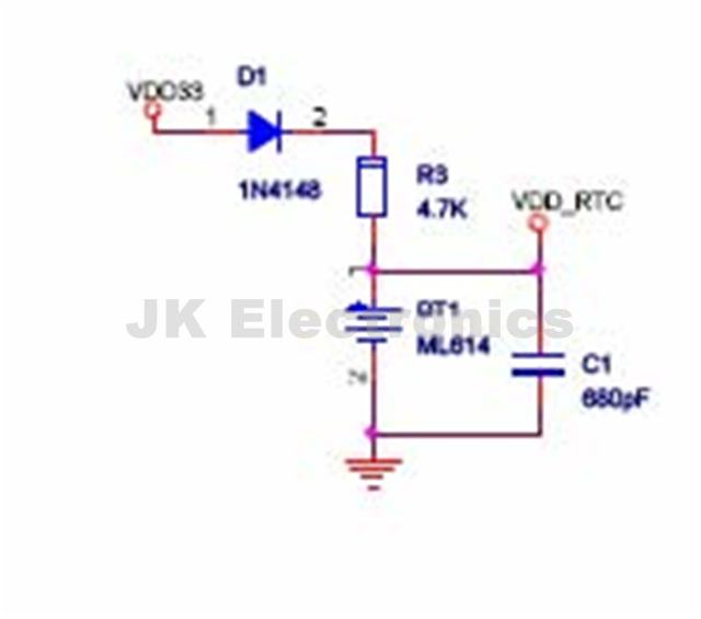
(5) VRTC power supply (1.8V ~ 3.0V)
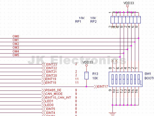
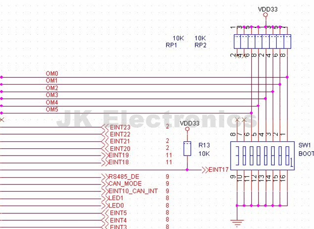
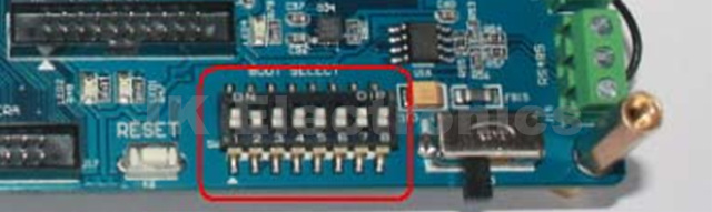
(6) BOOT configuration switch (UART-based boot and NAND boot)
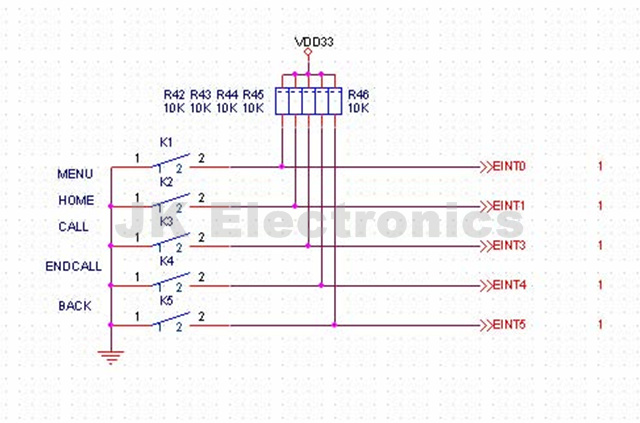
(7) User Button
각각의 버튼들은 CPU보드의 외부 핀에 EXTI 핀 기능으로 모두 연결 되어 있습니다.
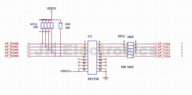
(8) KEYPAD matrix keyboard
모두 100R 풀업 저항으로 연결 된 5*5 매트릭스 키패드 인터페이스를 제공 합니다.
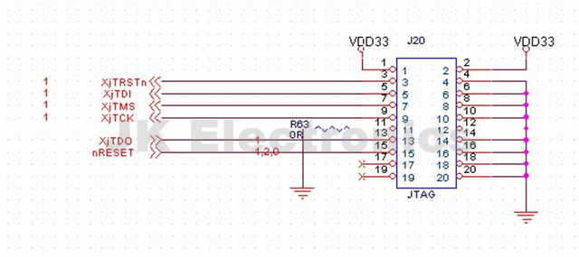
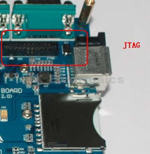
(9) JTAG Interface(20핀)
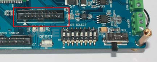
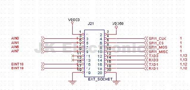
(10) External expansion interface
- 4개의 ADC input
- 2개의 외부 인터럽트 핀
- all the way SPI1 channel
- UART3 and UART1( TTL level serial port)
- 3.3V, 5V 전원, GND
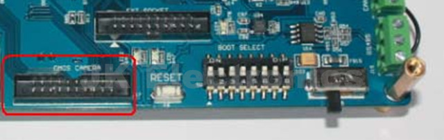
(11) Camera interface
(12) CAN interface
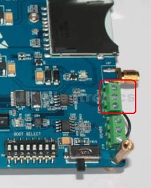 위에서 아래로 CANL, CANH, GND
 (13) RS485 interface
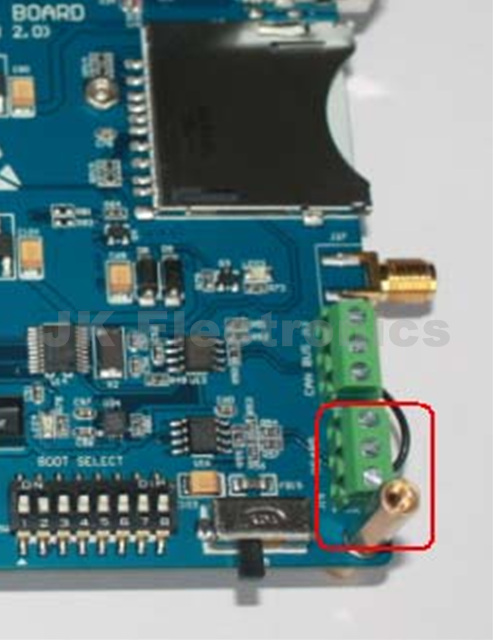 위에서 아래로 GND , B, A
(14) Audio 입/출력
- 1개의 MIC입력과 2.5 파이 Line in 인터페이스
- 2.5파이 헤드폰 출력 인터페이스
- 1.5W 스피커 출력 단자
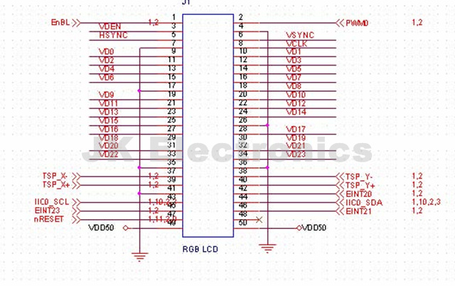
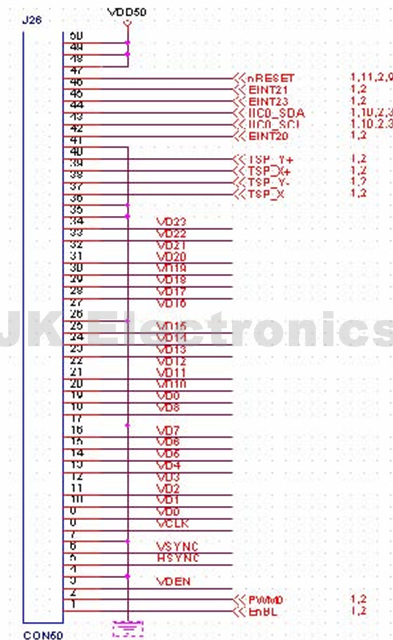
(15) RGB display output interface
개발보드에느 2개의 RGB output 인터페이스가 있지만, 2개중에서 1개만 선택해서 사용해야 합니다. 즉 2개의 인터페이스에 동시에 출력이 나오지 않습니다.
 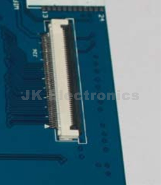 |
FPCB 인터페이스 |
 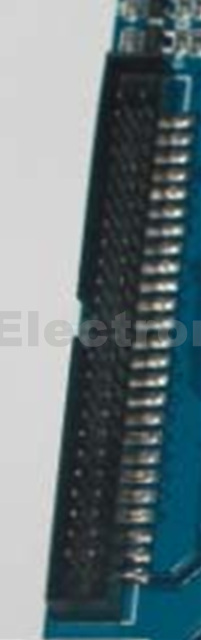 |
커넥터형 인터페이스 |
(15) GPS module
모듈 사용시 GPS 모듈은 별도 문의 바랍니다.
(16) Mini PCI 타입의 CDMA 모뎀
모듈 사용시 CDMA 모뎀 별도 문의 바랍니다.
(17) SDIO Wifi
모듈 사용시 SDIO Wifi 별도 문의 바랍니다.
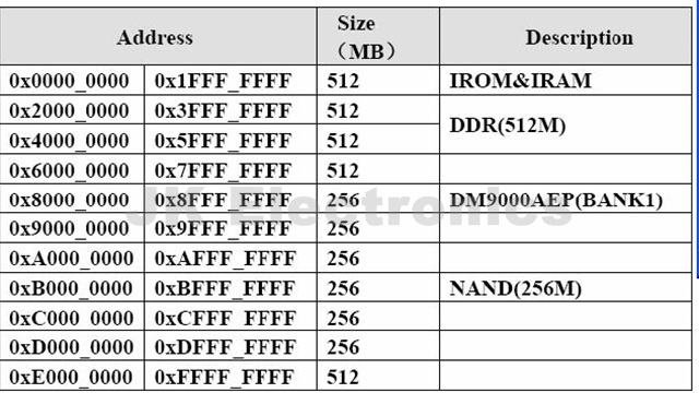
3. S5PV210 BOOT Memory layout
3.1 S5PV210 BOOT Configuration
S5PV210는 여러 장치에서의 BOOT옵션을 제공합니다. S5PV210 StartKit 개발보드에서는 UART, NAND, SD Memory 3개의 BOOT 옵션을 지원 합니다.
아래 표에서 OM0 ~ OM5 부트 옵션 참조하시기 바랍니다.
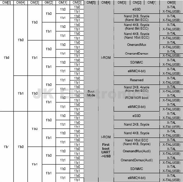
개발보드 BOOT옵션 회로도와 BOOT DIP 스위치
3.1.1 S5PV210 UART boot process
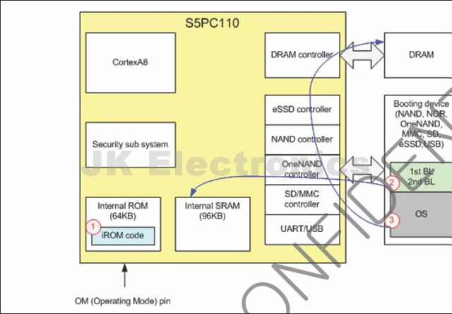
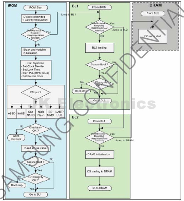
- iROM code : S5PV210 내부의 프로그램 ROM에서 동작하는 코드 입니다. Serial Port 로 Start할 경우에 동작 합니다. 이 코드는 internal 96K SRM BOOT 영역에 다운로드 되고 1st Bootloader를 실행 시킵니다.
- 1st Bootloader : USB를 초기화 시키고, 2nd Bootloader를 실행 시킵니다.
- 2st Bootloader : OS 이미지등을 Nand FLASH 영역에 다운로드 시키고 실행 시킵니다.
위의 내용을 좀더 자세히 살펴보면 다음과 같습니다.
3.2 Memory layout